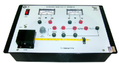
Thermistor Characteristic Apparatus (ME 546D)
Symbol diagram printed on Aluminum Front Panel & all important test Points are brought out on front panel.
Product Overview
Symbol diagram printed on Aluminum Front Panel & all important test Points are brought out on front panel.
Symbol diagram printed on Aluminum Front Panel
& all important test Points are brought out
on front panel.
Temp. Vs resistance at different voltages.
Voltage Vs current at different temperatures.
Current Vs time at different voltages
Output Voltage : 0-10 VDC
Voltmeter : 0-10 VDC
Ammeter : 0-500MicroADC
For more details please refer datasheet.
Technical Specifications
Symbol diagram printed on Aluminum Front Panel
& all important test Points are brought out
on front panel.
Temp. Vs resistance at different voltages.
Voltage Vs current at different temperatures.
Current Vs time at different voltages
Output Voltage : 0-10 VDC
Voltmeter : 0-10 VDC
Ammeter : 0-500MicroADC
For more details please refer datasheet.
Talk To Our Technical Experts
Related Products
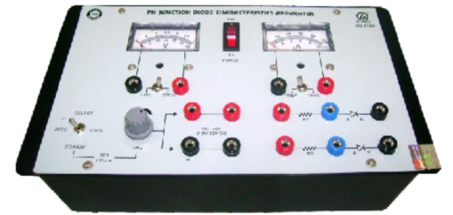
PN Junction Diode Characteristics Apparatus (ME 539D)
PN Junction Diode Characteristics Apparatus is analog electronic lab equipment
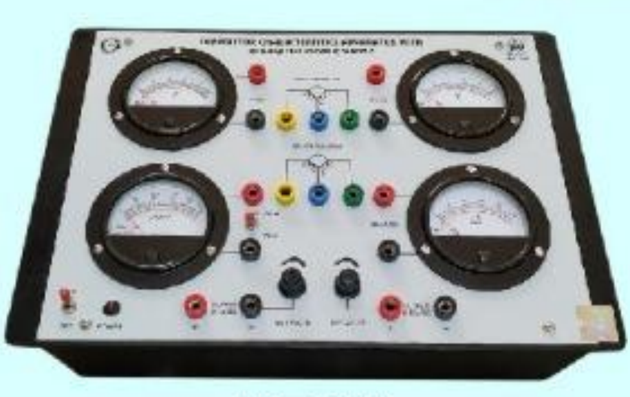
Transistor Characteristics Apparatus (ME 533)
Plot the input, output and transfer characteristics of PNP & NPN transistors in common emitter & common base configuration.
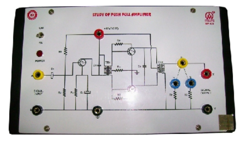
Push-Pull Amplifier (ME 620)
Push-Pull Amplifier Apparatus has been designed to study the Output Gain, Output Power and Frequency Response of a Push Pull Amplifier
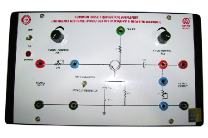
Common Base Transistor Amplifier (ME 617)
Common Base Transistor Amplifier apparatus with and without Negative Feed Back has been designed to study the following :- A. Frequency Response / Output Voltage Gain. B. Input Impedance. C. Output Impedance. D. Effect of Negative Feed Back on Output Gain